100 MHz
PCBITE-6013
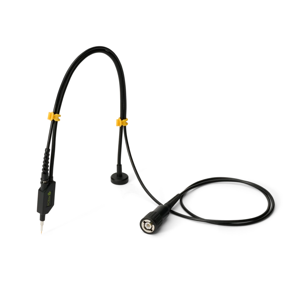
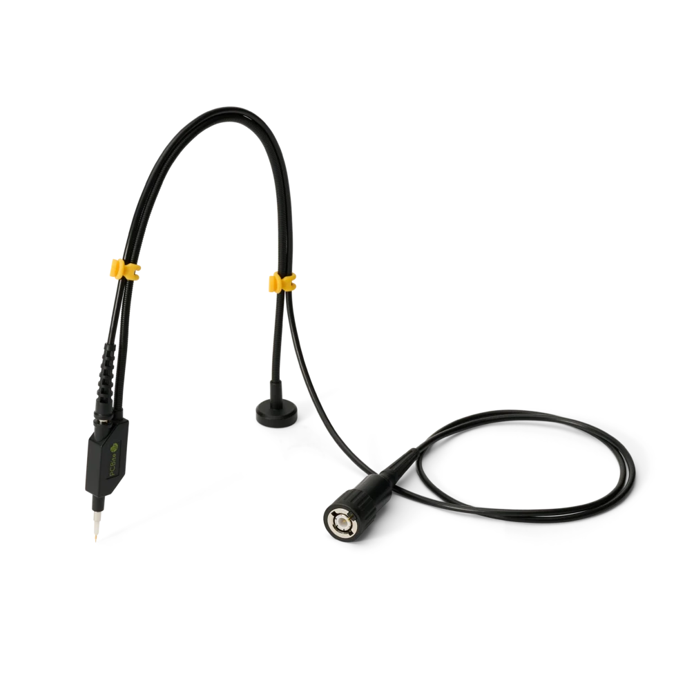
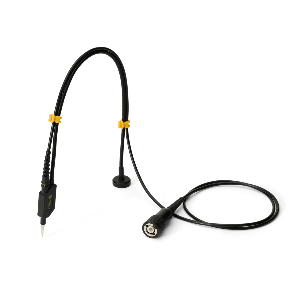
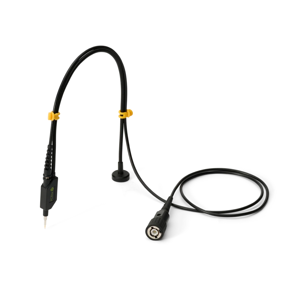
SQ100 – 100 MHz handsfree oscilloscope probe
59 €
In stock
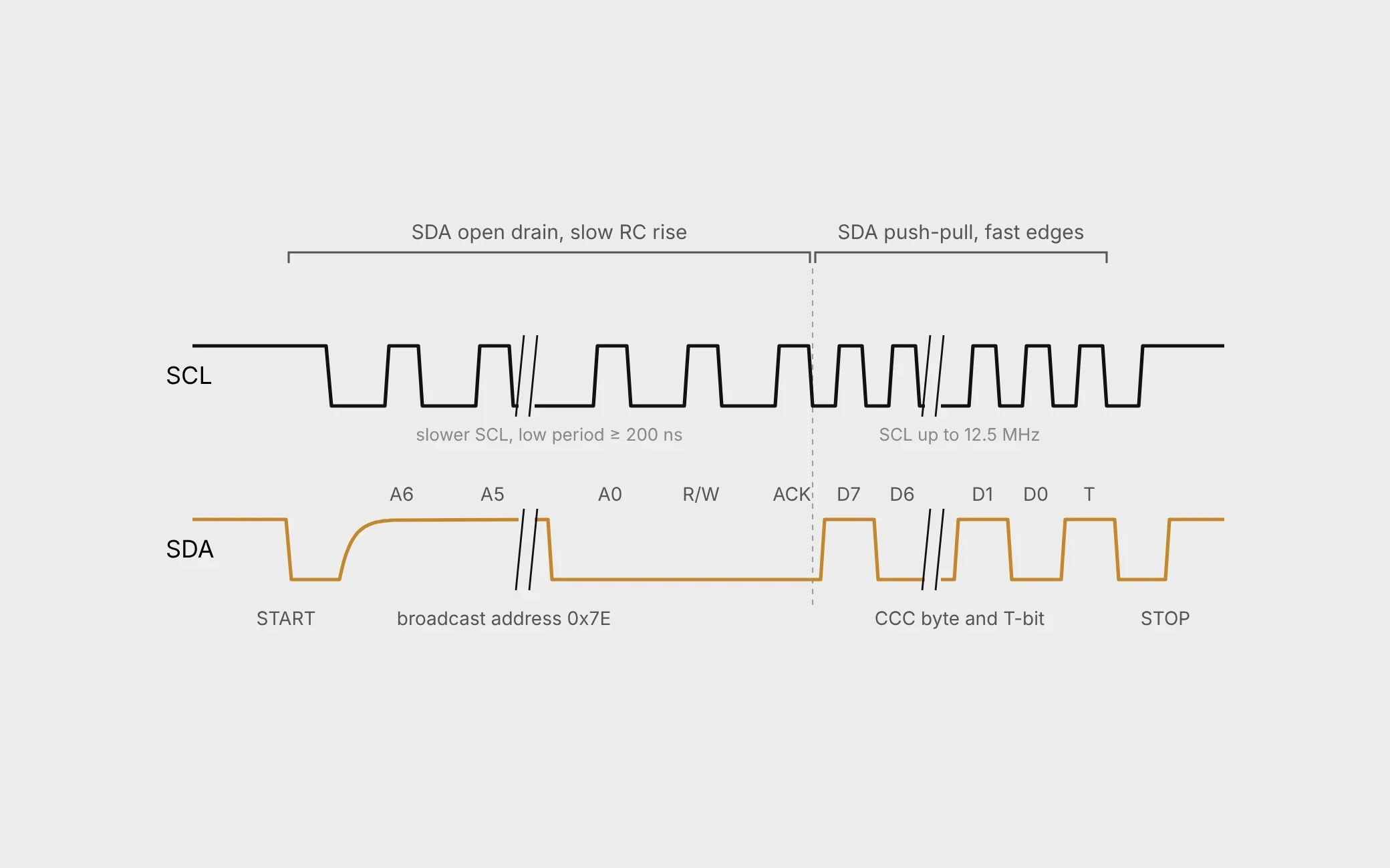
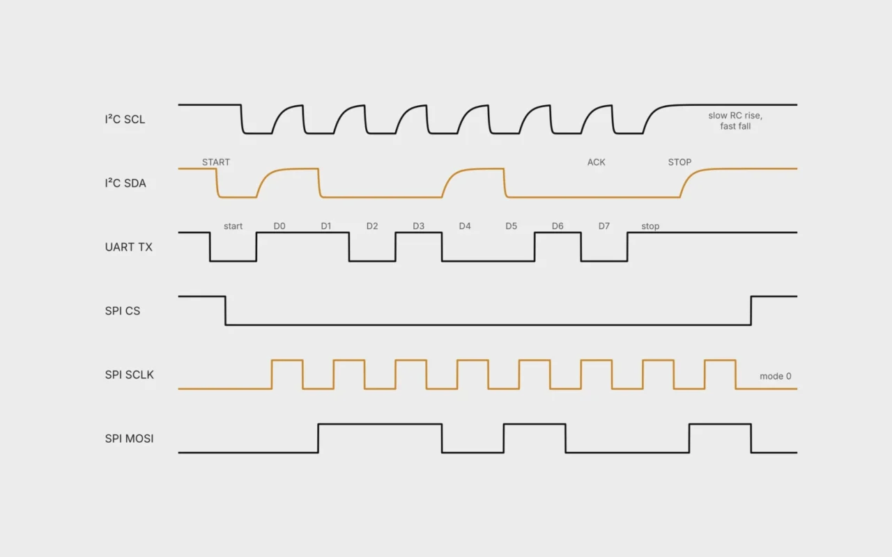
Fig. 1. An I3C frame in SDR (single data rate) mode. After a START the address header is driven open drain, with slow RC rising edges on SDA. From the first data bit the controller drives SDA push-pull, and the ninth bit of each byte is a T-bit (transition bit) instead of an ACK. SCL is always driven push-pull. Illustration.
I3C was developed by the MIPI Alliance as a two-wire bus for peripherals1, from sensors and actuators to power regulators and microcontrollers2, 3. I3C Basic is the royalty-free version that anyone can download2. It is used as the sideband bus on DDR5 memory modules and as a management bus for SSDs4, and it is found in MEMS sensors from Bosch, STMicroelectronics and TDK InvenSense and in microcontrollers such as the STM32H5 and the Microchip PIC18F16Q205, 6.
Like I2C, I3C uses the two lines SDA and SCL, and legacy I2C devices can share the bus as long as they do not stretch the clock. I2C devices with a 50 ns spike filter let the bus run at full I3C speed, while devices without one limit it to I2C speeds1, 3. What I3C adds is dynamic addressing, in-band interrupts that replace separate interrupt pins, hot-join for devices that power up late, and much higher speed.
In SDR (single data rate) mode the clock runs at up to 12.5 MHz, which gives 12.5 Mbit/s raw and about 11 Mbit/s in practice3. The optional HDR (high data rate) modes go further. HDR-DDR changes data on both clock edges and reaches 25 Mbit/s at the same clock2, HDR-BT is made for bulk transfers, and multi-lane transfers add up to three extra data lines1. I3C Basic is specified for 1.2 V, 1.8 V and 3.3 V and is not characterized for 5 V. An optional variant, used on DDR5 memory modules, runs at 1.0 V with up to 100 pF1.
Every I3C frame starts with a START and an address header that works like I2C1. In this first header SDA is open drain: always for the first address bit and the ACK, and normally for the whole header. Devices pull the line low, and a pull-up in the controller brings it high, so the rising edges are slow RC curves. This lets several devices transmit at the same time, which is how a target requests an in-band interrupt or a hot-join, and the lowest address wins the arbitration1. SCL is never open drain; the controller always drives it push-pull. An address sent after a repeated START is push-pull too, apart from its ACK bit, unless it is addressed to a legacy I2C device1.
After the ACK the controller switches SDA to push-pull, and both edges become fast1. The ninth bit of each byte is a T-bit, not an ACK. On a controller write it carries parity; on a read it lets the target end the transfer and the controller abort it1. The open-drain pull-up is switched off during push-pull, and a weak high-keeper holds the lines high whenever nobody drives them1.
On a mixed bus with I2C devices, the controller hides the fast traffic from them. The SCL high period, measured between the input thresholds, is kept at 45 ns or less, shorter than the 50 ns spike filter in each I2C device, so the I2C devices see SCL as permanently low1, 7. The controller can still run slower by making the low period longer. The first broadcast address after power-up is sent with a high period of at least 200 ns, so that I3C targets that start with an I2C spike filter can detect the I3C bus and turn the filter off1.
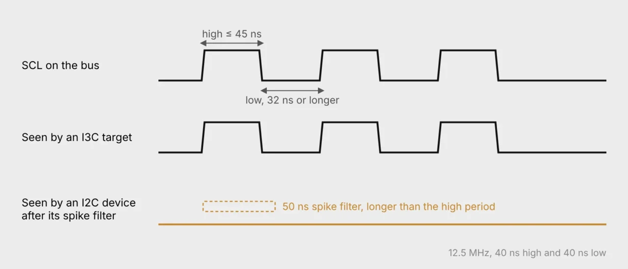
Fig. 2. SCL on a mixed bus. The high period is shorter than the 50 ns spike filter in the I2C devices, so an I3C target sees the clock and an I2C device sees a line that stays low. Illustration.
HDR modes are entered with a broadcast command and left with an exit pattern of four falling SDA edges while SCL stays low1. To a decoder that only knows I2C, this pattern looks like noise.
The I3C specification limits each bus line to 50 pF at full speed and allows each device pin up to 10 pF at 1.8 V and above, and 5 pF below 1.8 V1. A 10:1 passive oscilloscope probe adds about 10 pF, roughly a fifth of the whole budget. The effect is different in the two halves of the frame.
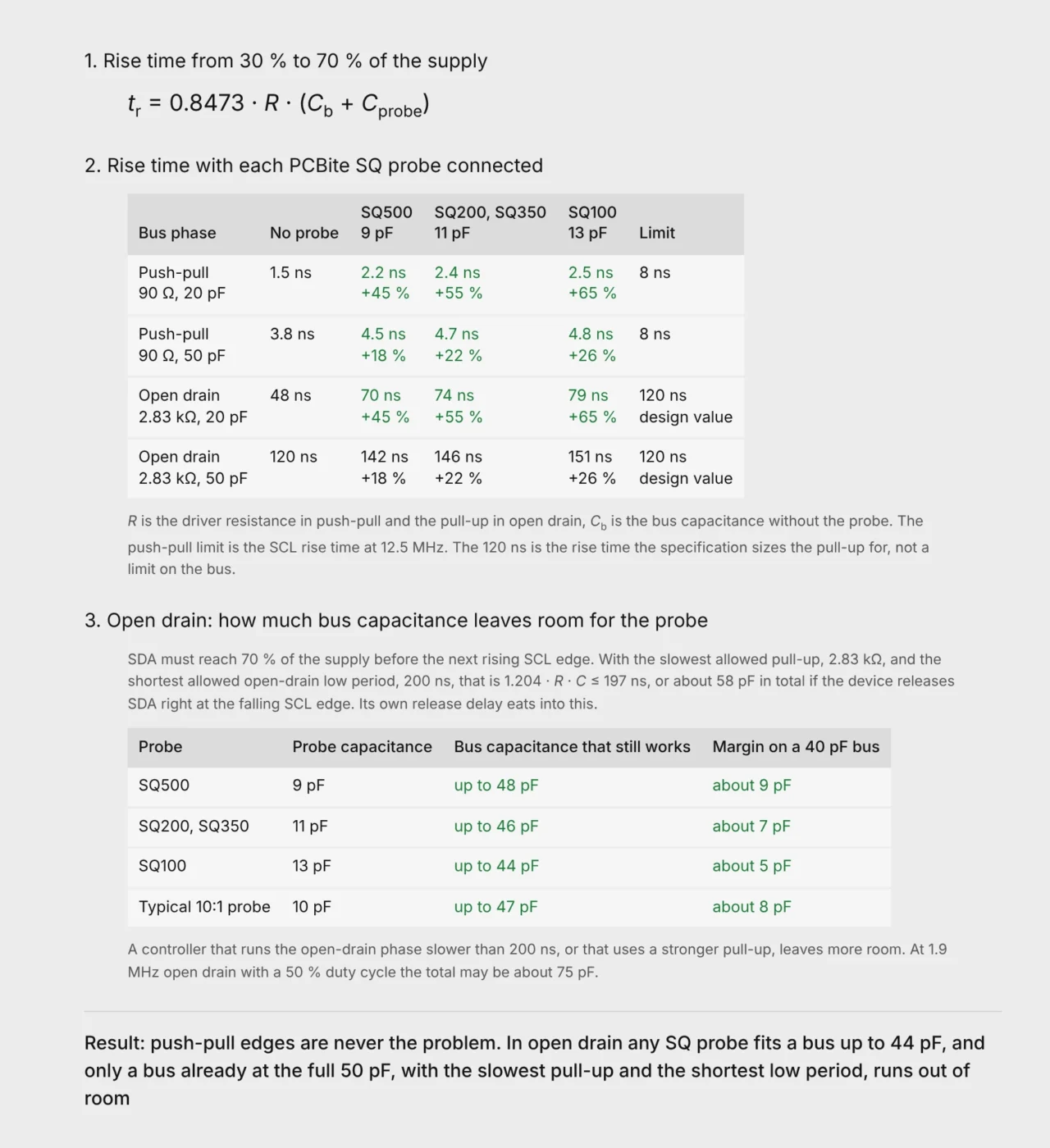
Fig. 3. Rise time from 30 % to 70 % of the supply with each PCBite SQ probe on the bus, for the push-pull and the open-drain phase, and the bus capacitance that still leaves room for the probe in open drain. Green values are within the limit.
Push-pull uses the 90 Ω driver that the specification assumes for its pad-delay figures. Open drain uses the 2.83 kΩ pull-up that the specification derives for 120 ns at 50 pF1.
Push-pull edges have plenty of margin, even when a probe adds a quarter or more to the capacitance. The open-drain phase is where a probe can be felt, so it is worth adding up what a real bus is. The specification allows 10 pF per device pin at 1.8 V and above and 5 pF below 1.8 V1, and a 50 Ω trace on FR-4 has about 1.3 pF per cm (3.3 pF per inch)8. A controller, two sensors and 10 cm (4 in) of trace therefore add up to at most 43 pF at 1.8 V or 3.3 V, and at most 28 pF on a 1.2 V bus, with every pin at its worst-case value. A bus like this sits well below 50 pF.
The 120 ns in Fig. 3 is the rise time the specification sizes the pull-up for, not a limit on the bus. The hard requirement is that SDA reaches 70 % of the supply before the next rising SCL edge. With the slowest allowed pull-up, 2.83 kΩ, and the shortest allowed open-drain low period, 200 ns1, that works up to about 58 pF in total, less the time the driving device needs to release SDA after the falling SCL edge. Only a bus that already sits at the full 50 pF runs out of room, and even then it accepts about 8 pF. Every picofarad below 50 pF goes to the probe: at 44 pF any SQ probe fits, and on a 40 pF bus the 13 pF SQ100 still has about 5 pF of margin. On a mixed bus the I2C devices see the open-drain header too, so keep their rise time limits in mind there, 300 ns for Fm and 120 ns for Fm+1. Controllers that run the open-drain phase slower than the minimum, as most do (STMicroelectronics gives up to 4 MHz, with about 1.9 MHz in its own example9), or that use a stronger pull-up, leave far more room. If address headers or ACKs fail only while the probe is connected, the bus is at that corner. Use the probe with the lowest capacitance, and check the open-drain phase first.
Balance between the lines matters too. The specification limits the capacitance difference between the SDA and SCL pins of a device to 1.5 pF, or 3 pF for pins above 5 pF1. A single probe adds 9 pF to 13 pF to one line only, so when the timing between SCL and SDA matters, probe both lines with the same probe model.
Timing is a digital question. Does the clock stay at or below 12.5 MHz, with only short bursts up to 12.9 MHz1? Do START, address, ACK, T-bit and STOP come where they should? Are dynamic addresses assigned, are in-band interrupts acknowledged, and do HDR transfers start and end correctly? A logic analyzer with an I3C decoder answers this.
Signal quality is an analog question. The low level must stay below 30 % of the supply and the high level above 70 %, and the inputs have at least 10 % hysteresis1. At 12.5 MHz, SCL may take at most 8 ns from 30 % to 70 % of the supply. That is the general rule of 10 % of the clock period, capped at 60 ns for slow clocks1. Open-drain falling edges on SDA must be faster than 12 ns1. The specification treats swings from −10 % to 110 % of the supply as normal overshoot and undershoot. Beyond that the input protection takes over, so check the absolute maximum ratings in the device data sheet1.
Read turnaround is where the two meet. When the controller reads, the target drives SDA after each falling SCL edge, and the controller samples it on the next rising edge. The internal clock-to-data delay of the target, tSCO, is normally at most 20 ns. Slower targets must report their delay to the controller. Delays in pads and wires add to this1. Version 1.2 of the specification raised the tSCO limit from 12 ns and tightened the SCL rise time at 12.5 MHz from 12 ns to 8 ns, so data sheets written to v1.1.1 still show the older values1. MIPI notes that with 1 m (39 in) between controller and target, reads work only up to about 6 MHz3. Measure SCL and SDA at the controller, with the same probe model on both lines.
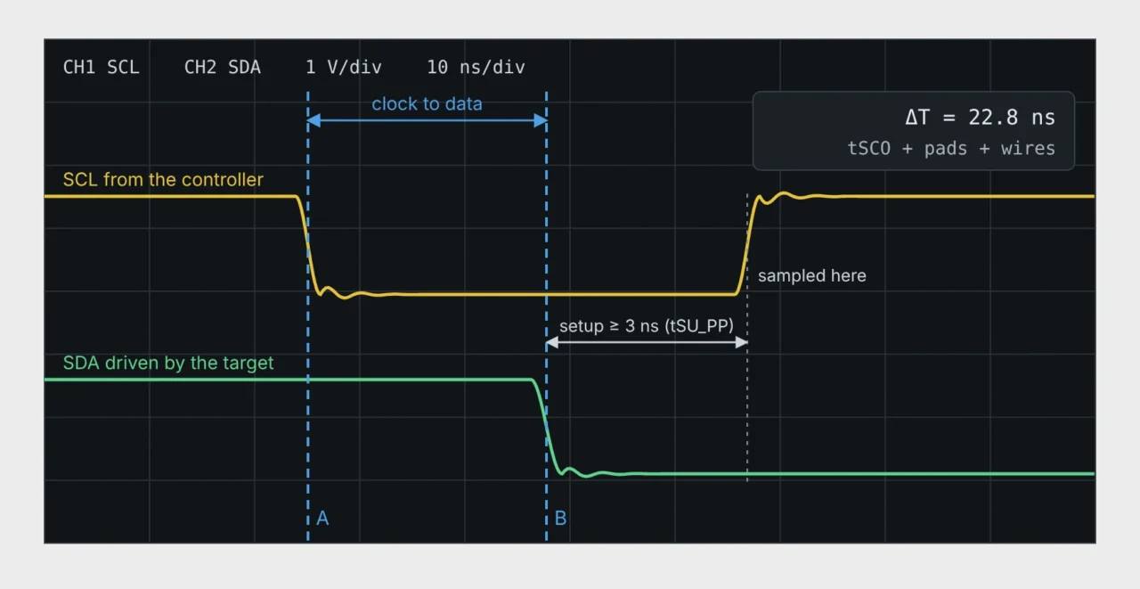
Fig. 4. Read turnaround seen at the controller. The time from the falling SCL edge to the SDA change includes tSCO of the target and the delays in pads and wires, and SDA must be stable at least 3 ns before the next rising edge. Illustration.
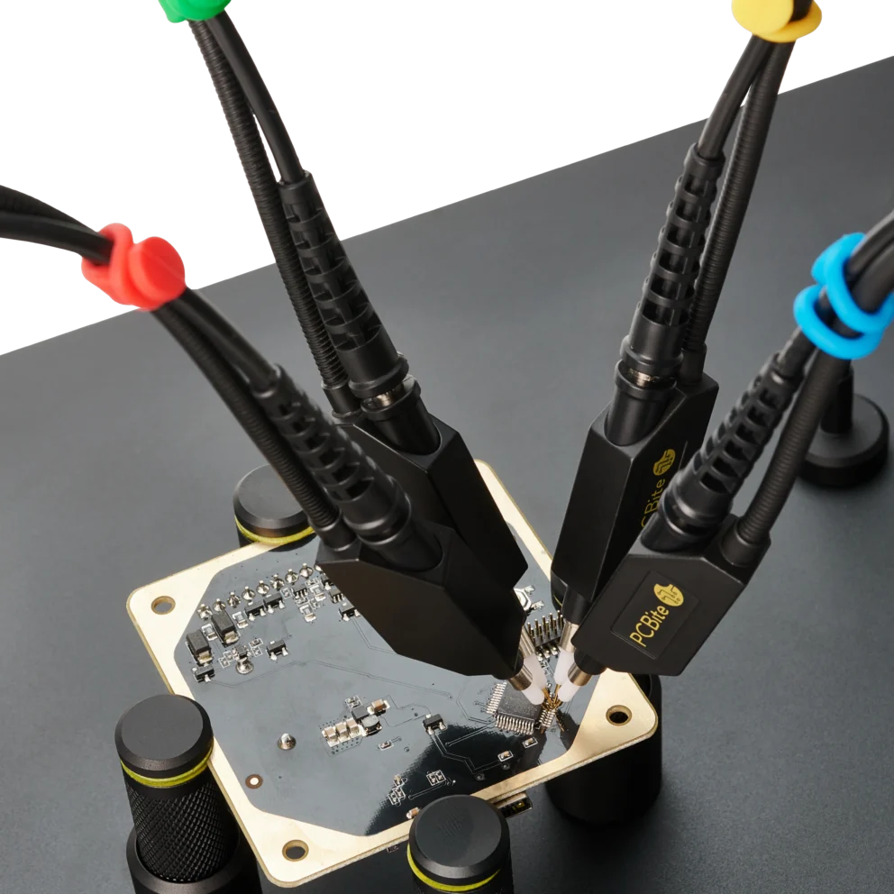
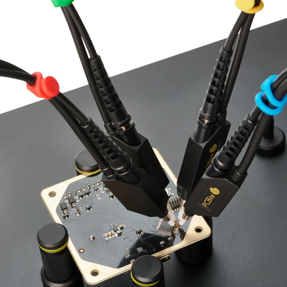
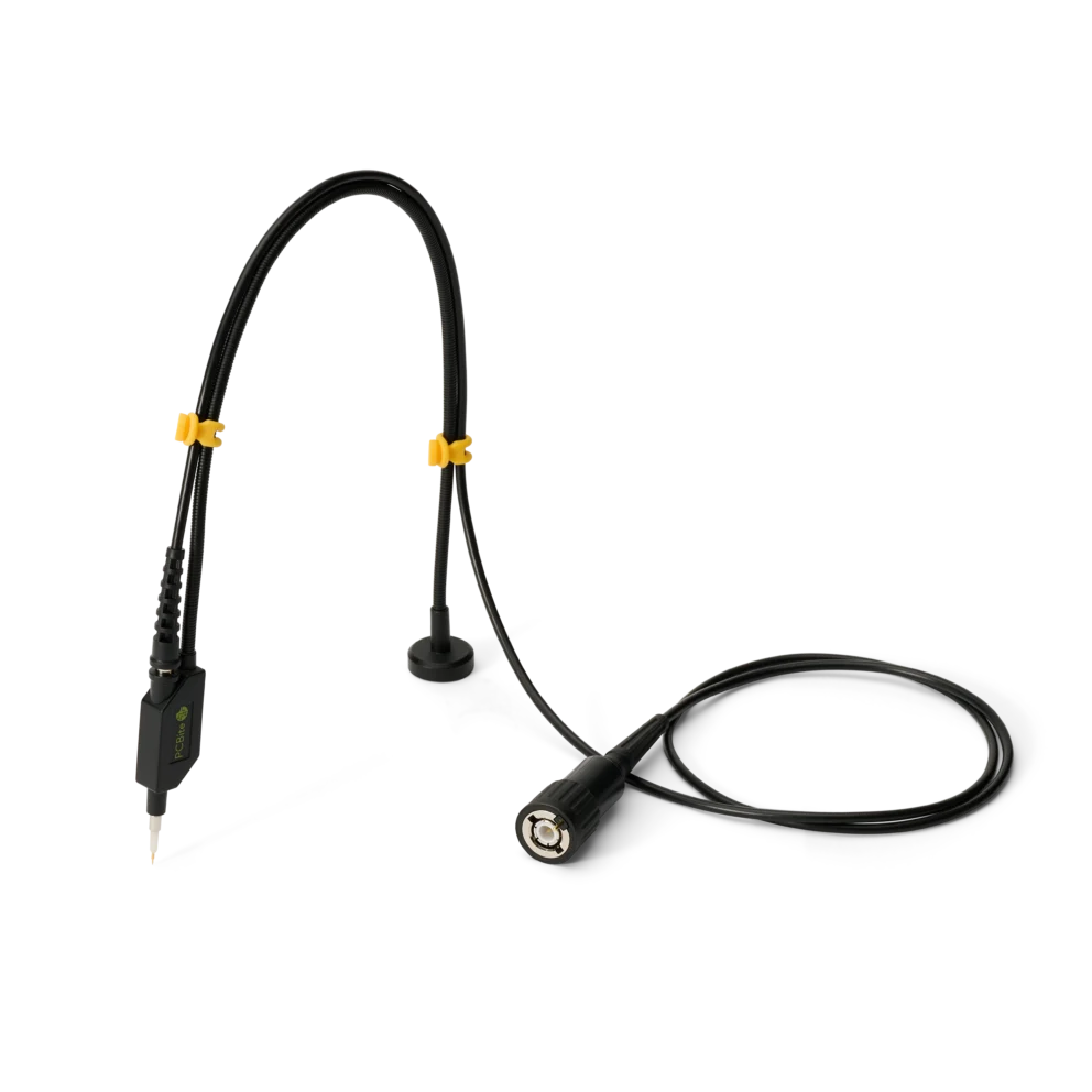
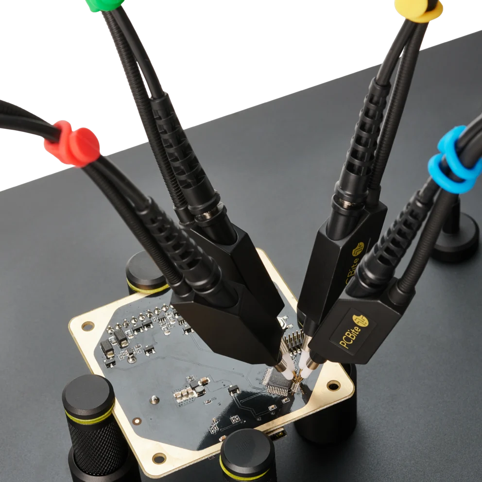
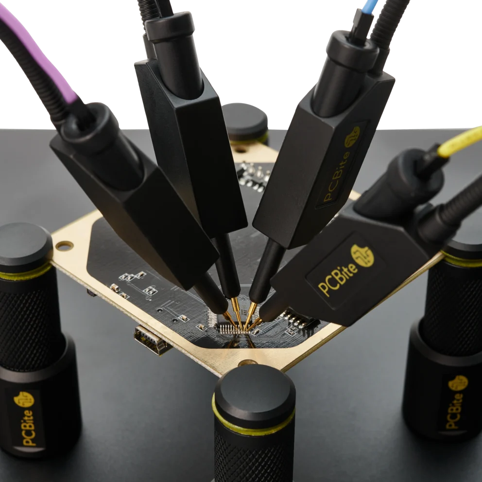
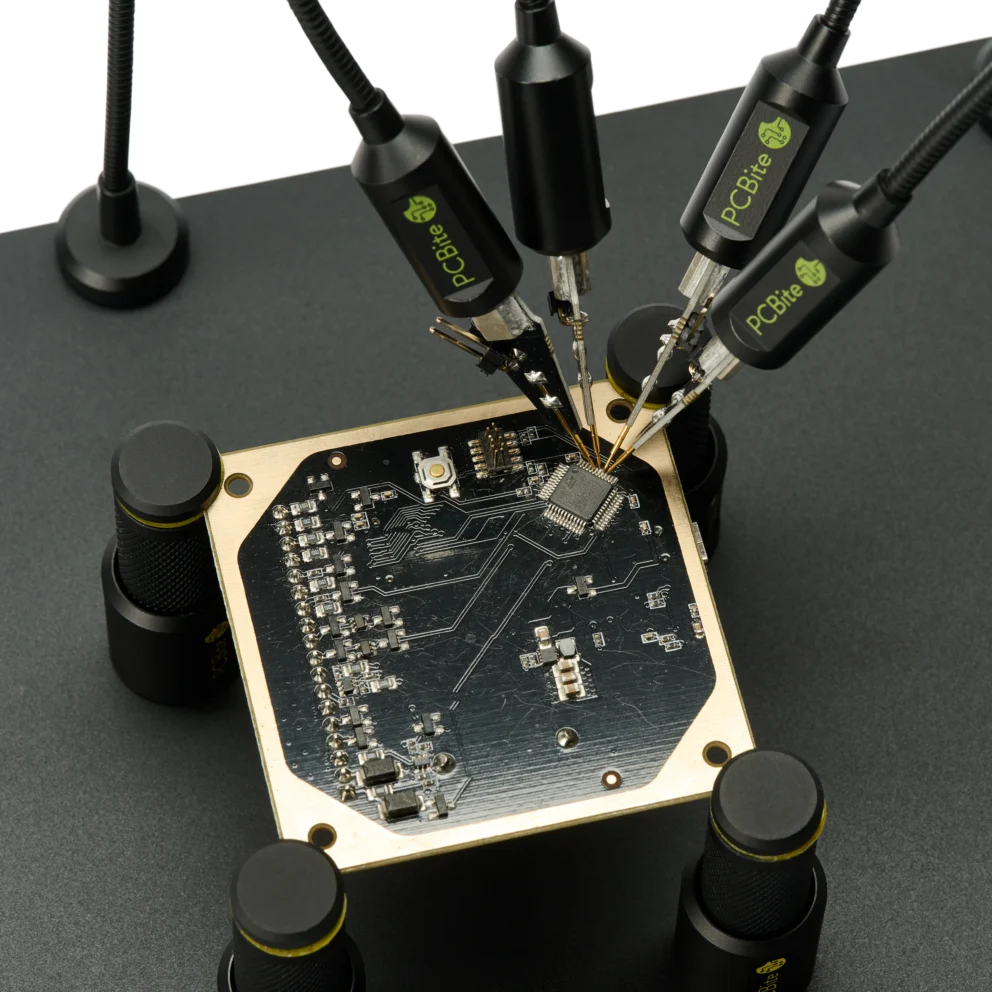
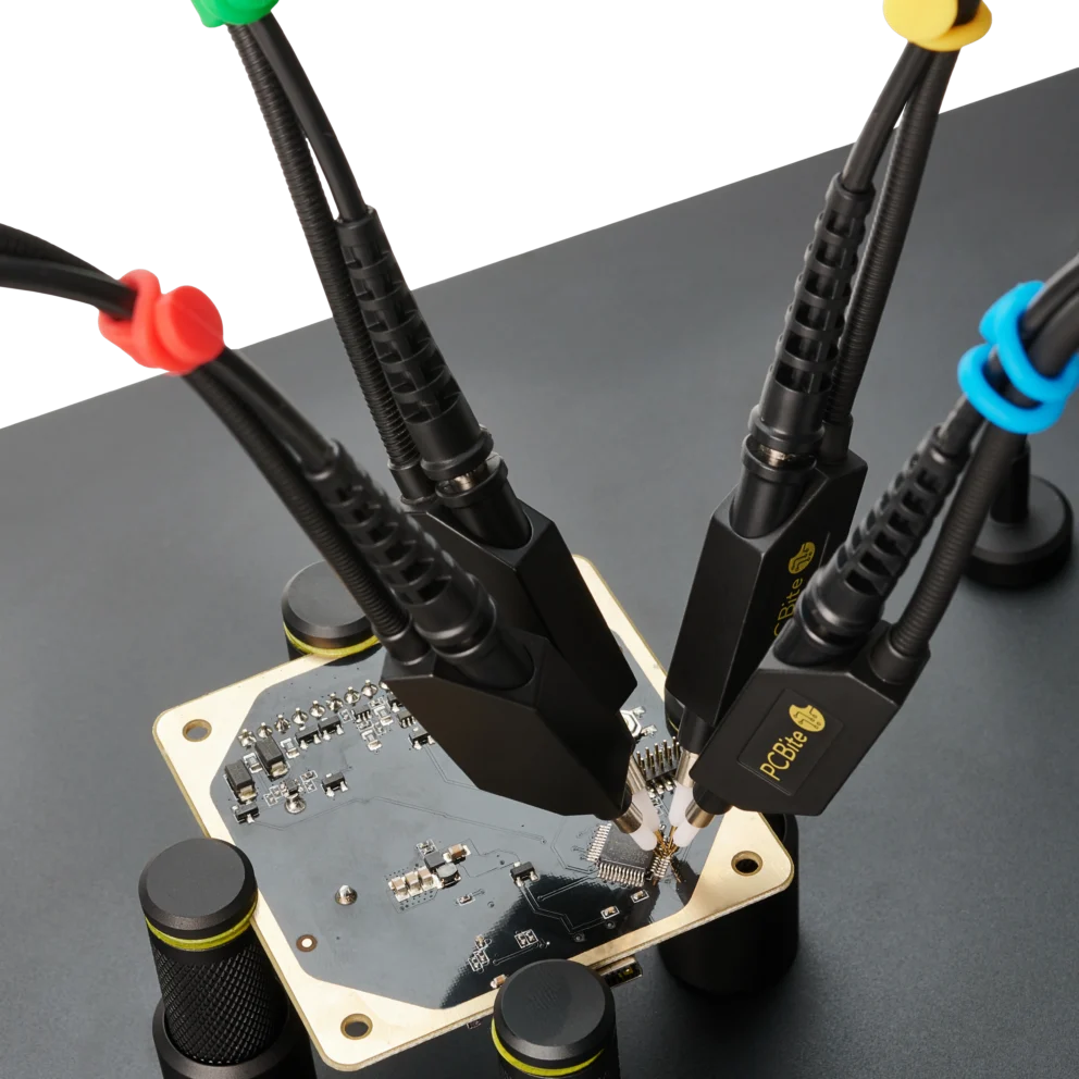
A 10:1 passive oscilloscope probe with an input resistance of 10 MΩ is the right tool10. It does not load the weak high-keeper or the open-drain pull-up. The PCBite SQ100, SQ200, SQ350 and SQ500 are 10:1 handsfree oscilloscope probes with bandwidths from 100 MHz to 500 MHz, 10 MΩ and 9 pF to 13 pF at the needle11. Sensepeek’s patented spring-loaded ground keeps the ground path short while the probe stays on the test point. Low-impedance probes such as the PCBite SQG series are the wrong tool here. They are made for a 50 Ω oscilloscope input and GHz edges. The DC-coupled models have a 380 Ω to 550 Ω path to ground that would pull an open-drain high level down to roughly 15 % to 50 % of the supply, depending on the pull-up, well below the 70 % input threshold, and the AC-coupled models load the edges just as heavily.
Push-pull edges on I3C are fast. With the 90 Ω driver that the specification assumes for its pad-delay figures, a 50 pF bus gives about 10 ns from 10 % to 90 %, and a short bus with 20 pF about 4 ns. Strong drivers on small boards can be faster still. The probe and the oscilloscope add their own rise time to the signal, and the measured value is approximately the square root of the sum of their squares12.
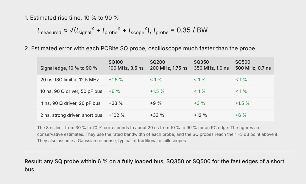
Fig. 5. Estimated error when the rise time of an I3C edge is measured with each PCBite SQ probe. Green values are within 6 %.
Our article on system bandwidth explains how probe and oscilloscope combine.
On a fully loaded 50 pF bus every SQ probe measures the edge within 6 %. On a short bus with fast edges, choose the SQ350 or SQ500. There the probe’s own capacitance changes the edge more than its bandwidth does (Fig. 3). The SQ500 has the lowest capacitance, 9 pF, and the fastest rise time, so it disturbs the bus least and shows the edge most accurately11.
The ground connection matters as much as the bandwidth. A ground lead adds inductance and a loop that picks up noise10, 13. In Sensepeek’s tests with the 170 mm (6.7 in) alligator ground cable the gain rises sharply above about 15 MHz, which shows up as false overshoot and ringing. That is close to the I3C clock itself, so use the ground spring needle for every I3C edge measurement. The SQ probes are tuned for a flat frequency response with it and reach their full rated bandwidth in handsfree use11.
A logic analyzer records ones and zeros on many channels and decodes them, and a mixed signal oscilloscope (MSO) adds analog channels to the same capture14. Binho’s I3C Basic Protocol Analyzer is a plugin for Saleae Logic that decodes SDR, HDR-DDR and HDR-BT, common command codes (CCCs), in-band interrupts, hot-join and multi-lane transfers, for I3C Basic v1.0 to v1.215. It runs on the Logic Pro 8, the Logic Pro 16 and the Logic MSO, and on the Logic 8 for buses at 1.8 V and above15.
Each SDR bit lasts 80 ns at 12.5 MHz, but the SCL high period can be as short as 32 ns, measured between the input thresholds1. Binho lists both the 500 MS/s of the Logic Pro models and the 100 MS/s of the Logic 8 as sufficient for 12.5 MHz I3C16. Use the highest rate available, especially for HDR-DDR, where data changes on both clock edges, and enable only the channels you need, since the Logic Pro reaches its top rate with few channels active17. Set to their 1.2 V threshold, the Logic Pro inputs switch at 650 mV ±15 %, and Binho recommends that setting for all bus voltages16. The threshold of the Logic MSO can be set from 0.6 V to 3.1 V14. Keep any glitch filter well below 32 ns. A 50 ns filter does exactly what an I2C spike filter does and hides the I3C clock. In the Logic 2 software the filter is applied at capture time and cannot be changed afterwards, so capture SCL and SDA without it18.
The logic analyzer is part of the bus load too. A Logic Pro 16 input has 10 pF17 and the digital probe of the Logic MSO 3 pF or less14, plus the cable. Decode on the digital channels, find the transfer that failed and look at the analog edge behind it.
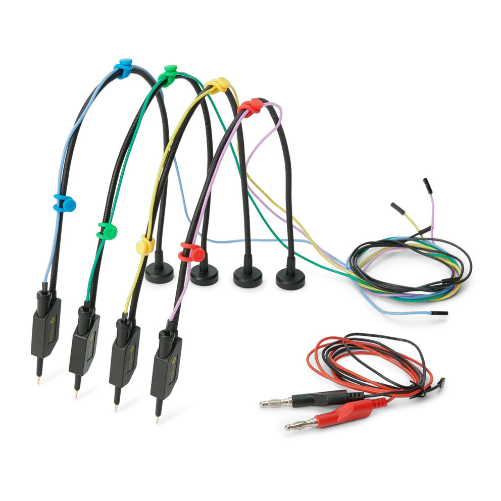
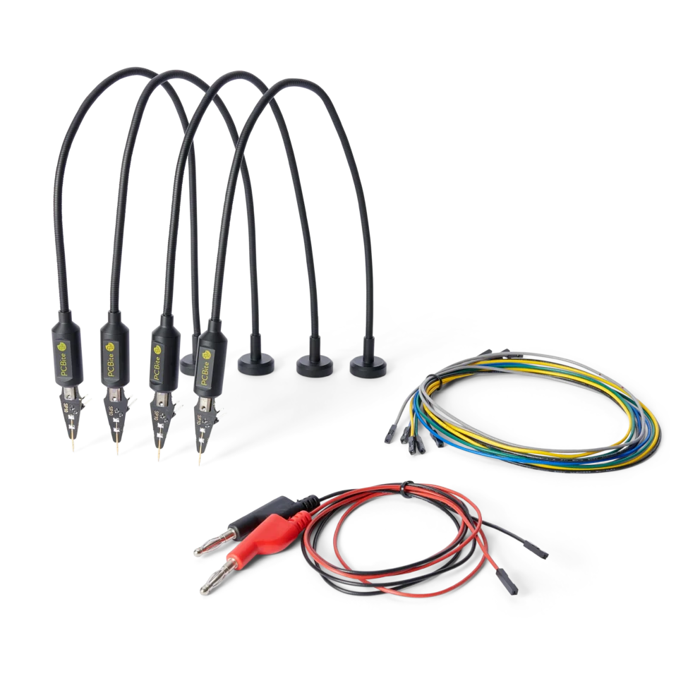
The PCBite SP10 and SQ10 are 1:1 handsfree probes for logic analyzers and MSO digital channels19. They connect with 2.54 mm (0.100 in) jumper connectors, often called Dupont connectors, and hold a needle on each test point without soldering. With the included 0.8 m (31 in) test cables they are rated for signals up to 10 MHz, below the 12.5 MHz of I3C. At 0.8 nH to 1 nH per mm (20 nH to 25 nH per inch)13, 20, a 0.8 m wire and the 10 pF input of a typical logic analyzer17 have, as a rough estimate, a first resonance around 50 MHz to 70 MHz, in the range of the fifth harmonic of a 12.5 MHz clock. On an I3C bus, use the SP10 and SQ10 for power, ground, reset and interrupt lines and for legacy I2C traffic, and put the SQB1 described below on SCL and SDA.
Much I3C work is done with a USB host adapter instead of the product’s own controller. The Binho Supernova acts as the I3C controller or as a target, sends transfers from a PC at up to 12.5 MHz in SDR and HDR-DDR, and handles in-band interrupts, hot-join and all CCCs21. Microchip has named Binho an official development tool partner for its I3C microcontrollers6, and the Supernova is used in Microchip’s online I3C demo21.
The connection between the adapter and the board is then part of the bus, and it must carry traffic in both directions. The adapter drives SCL and SDA, and the targets drive SDA back. Jumper wires do this, but they add capacitance and inductance of their own, and they must be soldered or clipped to the board. A 10:1 oscilloscope probe cannot do it, because the 9 MΩ series resistor in its head blocks any drive current to the bus.
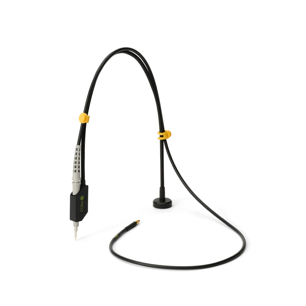
The PCBite SQB1 is a passive, bidirectional 1:1 probe made for this. It was commissioned by Binho and developed together with them for the Supernova, and it is the world’s first low-capacitance bidirectional handsfree probe for I3C22, 23. The probe’s measured capacitance is below 41 pF at 12.5 MHz22, 24, and Binho specifies the pack at a total capacitive load below 45 pF23. That leaves a few picofarads for a small board within the 50 pF the specification allows at full speed. A larger bus runs at reduced speed, and possibly without I2C devices, as the specification also allows1. The SQB1 is specified for push-pull traffic up to 12.5 MHz at 2.5 V to 3.3 V and up to 10 MHz at 1.8 V, and for open-drain traffic up to 3.12 MHz22. It is designed and tested with the Supernova and with Saleae Logic running Binho’s I3C analyzer plugin23. Its bandwidth is above 13 MHz in both directions and above 100 MHz one way, so the same probe also serves as a passive probe for the logic analyzer. Adapter boards connect its MMCX cable to the Supernova and to the Logic Pro 8 and Pro 1623. Use one SQB1 on SCL and one on SDA, so that both lines see the same load24.
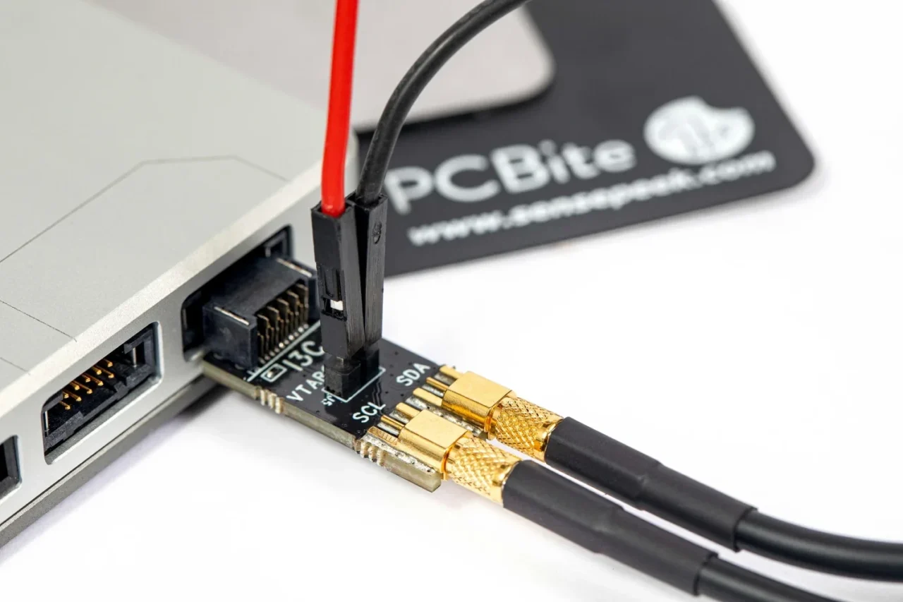
Fig. 6. The adapter board in the I3C port of the Binho Supernova. The two SQB1 probes connect to SCL and SDA through their MMCX cables, and the red and black cables on the VTARGET and GND pins lead to the SQ10 probes that power the circuit under test.
The probe head has 100 Ω in series and a coaxial design with signal and ground of equal length22. The spring-loaded signal and ground needles press with 60 g to 100 g, while a rigid probe presses with 400 g to 1 kg, so the board is loaded less and you feel when the needle makes contact22. Like the other SQ probes it has an insulated grip for handheld use and a magnetic probe holder that keeps it handsfree on a PCBite base plate, and it takes the same ground accessories, from the ground spring needle to clips with alligator or mini grabber cables24. It is made for digital serial interfaces such as I3C and I2C, not for analog measurements, and it is not designed for a 50 Ω or 1 MΩ oscilloscope input24.
Binho stocks the PCBite range and sells the SQB1 in two packs23. The Binho I3C Handsfree Probe Pack has two SQB1 probes for SCL and SDA, two SQ10 probes for power and ground, ground accessories, cable holders and adapter boards for the Supernova and Saleae Logic. It suits a bench that already has a PCBite kit. The Binho I3C Handsfree Probe Pack with PCBite Kit adds the PCBite kit L, with its A4 base plate, four PCB holders, insulation washers and insulation cover, for a complete second setup.
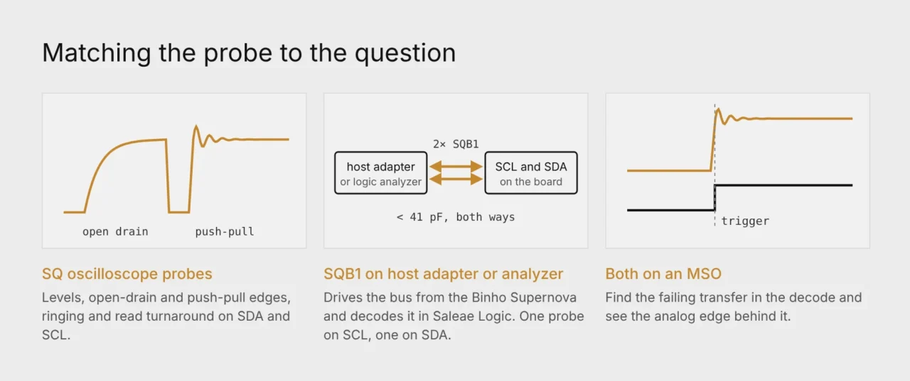
Fig. 7. The oscilloscope answers analog questions, the SQB1 connects the host adapter or the logic analyzer to the bus, and an MSO shows both views in one capture.
Pick the probe by the question. SQ oscilloscope probes show levels and edges. The SQB1 connects a host adapter or logic analyzer to SCL and SDA. SP10 and SQ10 handle power, ground and slower lines. Whatever you connect, keep the bus under 50 pF, use the same probe model on SCL and SDA, and use the ground spring needle for every edge measurement.
Du använder en föråldrad webbläsare. Alla funktioner fungerar inte i din webbläsare. Var vänlig uppgradera din webbläsare för att förbättra din upplevelse och öka din säkerhet.